
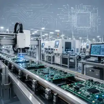
Semiconductor PTFE — Material Specifications, Engineering Data & OEM & ODM Supply
Built to international industrial standards, Semiconductor PTFE from HEMSUN delivers low friction and universal chemical inertness for semiconductor components. Fabricated in Dahegam, Gandhinagar, Gujarat, India from high-density PTFE fluoropolymer with full material certification.
Where Semiconductor PTFE is used
Specified for high-purity wet-bench and gas-line duty where ionic contamination and particle shedding must stay minimal.
Common in wet benches, chemical delivery modules and gas handling on fab equipment.
Key properties
In-house Semiconductor PTFE production
moulding and CNC under one roof
Drawing, CAD (STEP/IGES/DXF), or sample-based reverse engineering
PTFE grade options matched to chemical and thermal duty
Dimensional inspection with reports on request
IEC-registered exporter
worldwide packing and docs
Flexible MOQ
prototypes, pilot lots, recurring OEM supply
Specifications
| Property | Value |
|---|---|
| Component Type & Grade | Semiconductor PTFE (Specification Code HES-816) |
| Base Raw Material | PTFE fluoropolymer (Virgin FDA 21 CFR 177.1550 / Custom Filled) |
| Continuous Service Temp. | -200°C to +260°C (-328°F to +500°F) |
| Tensile Strength at Break | 20 to 35 MPa (Virgin) / 14 to 25 MPa (Filled) |
| Elongation at Break | 250% to 450% (ASTM D4894) |
| Specific Gravity / Density | 2.14 to 2.18 g/cm³ (ASTM D792) |
| Dielectric Strength | 50 to 80 kV/mm (0.1 mm film) |
| Surface Roughness Finish | Diamond Polished Ra ≤ 0.20 µm to Ra ≤ 0.40 µm |
| Dimensional Tolerance | ISO Grade 1 to Grade 3 / Drawing Nominals (±0.02 mm) |
| Manufacturing & Origin | Moulded, Sintered & CNC Machined in Dahegam, Gandhinagar, Gujarat, India |
Manufacturing process
Fabrication of Semiconductor PTFE relies on high-tonnage powder compaction and free sintering of PTFE fluoropolymer. Preforms are pressed under strict pressure dwell parameters, then heat-treated above 342°C in forced-convection ovens to bond resin granules into a void-free, chemically resilient matrix.
Material selection notes
Engineered from high-purity PTFE fluoropolymer, this component resists virtually all industrial acids, alkalis, and aggressive organic solvents. The non-stick, self-lubricating surface minimizes drag and prevents material buildup in fluid handling systems. Compressive deformation under load is optimized through tailored filler grades based on service pressure.
How to specify your order
Sizing and ordering Semiconductor PTFE: Share drawing files (STEP/PDF), annual volume projections, and any compliance requirements (FDA, USP Class VI). Our technical department confirms tooling costs, sample schedules, and volume production lead times.
Quality checks and inspection
Testing procedures for Semiconductor PTFE include optical comparator profile inspection, hydrostatic pressure holding tests on seal components, and material hardness checks (Shore D) to verify full sintering cure.
Ordering and export documentation
Domestic Semiconductor PTFE orders ship with GST invoice and e-way bill where applicable. Export orders include commercial invoice, packing list, and certificate of origin from our IEC-registered works. Recurring supply schedules supported with fixed drawing revision and lot numbering for plant stores Contact info@hemsun.com or sales@hemsun.com with your PTFE components specification. HEMSUN supports semiconductor equipment manufacturers with in-house design and fabrication of precision hydraulic preforming presses, fluoropolymer billet compression units, and custom cleanroom tooling fixtures. HEMSUN supports semiconductor equipment manufacturers with in-house design and fabrication of precision hydraulic preforming presses, fluoropolymer billet compression units, and custom cleanroom tooling fixtures.
Export packing and lead time
Export logistics for Semiconductor PTFE cover global delivery via air freight or ocean container through Mundra and Nhava Sheva ports. Products are packed with protective foam wrapping and moisture-barrier film inside export-grade wooden crates, accompanied by certified commercial invoices and Certificates of Origin.
Storage and handling
Handling and assembly guidelines for Semiconductor PTFE: Components should be kept in protective polybags until final assembly. Use clean, rounded assembly mandrels when installing over shaft threads to prevent surface scratches or edge nicking.
Compliance & Standards
IEC registered. Material certificates and dimensional reports available on request. Export documentation for commercial and project shipments worldwide.
Frequently Asked Questions
Why do semiconductor fabs specify PTFE components?
PTFE offers chemical inertness, low contamination risk, and stable dielectric properties for wet bench hardware, fluid handling, and precision spacers in semiconductor processing environments.
Can HEMSUN hold tight tolerances for semiconductor parts?
Yes. CNC machined PTFE components can be produced to drawing tolerances with deburred finishes suitable for precision electronic assembly.
Related Machinery, Tooling & Technical Guides
Manufacturing Presses
Engineering Process Guides
Related Products
Related Articles

Can PTFE Balls Be Used in Drinking Water Systems?
View DetailsChoosing the Right Ball Size for a Check Valve
View Details